Analysis and Suppression Strategies of the Influence of Power Ripple on Signals in Precision Measuring Instruments

Power ripple usually refers to the periodic AC component superimposed on the DC output, as well as random broadband noise. This article will delve into how power ripple degrades the accuracy and signal-to-noise ratio (SNR) of precision measuring instruments through conduction, radiation, and limited PSRR (Power Rejection Ratio) paths.
1、 The sources and characteristics of power ripple
Switching power supply ripple
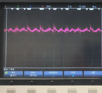
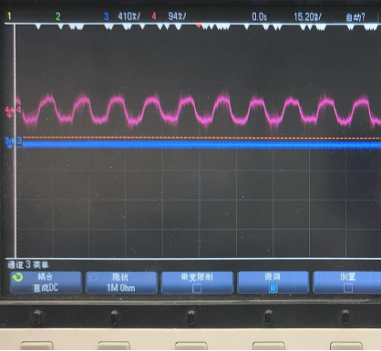
Features: Contains high-frequency switching frequency fundamental wave (usually 50kHz~5MHz) and its harmonics, as well as spikes caused by inductor current ripple.
Form: Typically presenting as sawtooth waves or square wave spikes with high-frequency damping oscillations. As shown in the figure:
power frequency interference
Characteristics: 50Hz/60Hz and its harmonics, mainly derived from the coupling of the mains or the introduction of the ground loop.
Form: Sine wave or distorted sine wave.
Transient response of load
Characteristics: When internal digital circuits (such as FPGA, MCU) or RF power amplifiers instantaneously draw large currents, the voltage drop and overshoot caused by the hysteresis response of the power feedback loop.
2、 Mechanism of action: How ripple "pollutes" signals
Limited power supply suppression ratio
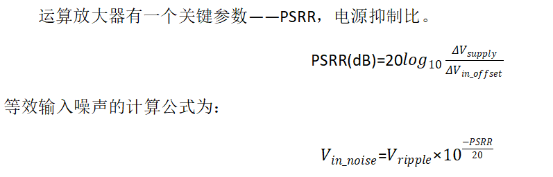
As shown in the figure, the PSRR frequency characteristic curve of precision operational amplifier AD823AARZ-R7.
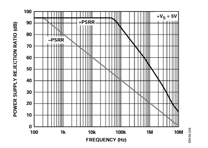
The curve shows that the PSRR can reach 90dB at low frequencies (<100Hz), and sharply decreases to 60dB as the frequency increases (>10kHz). This indicates that even small amplitudes of high-frequency ripple may be equivalent to larger errors.
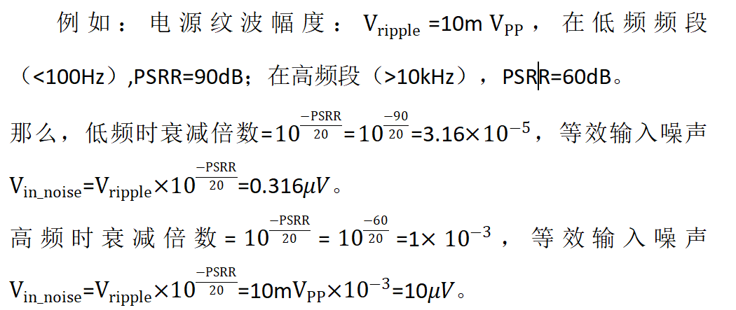
So, the equivalent input noise at high frequency increased from 0.316 μ V to 10 μ V, amplifying by about 31.6 times.
Interference and ground bounce
In a mixed signal system, the transient current of the digital part generates noise voltage through a shared power plane or ground plane impedance. This noise enters the analog front-end through capacitive coupling or common impedance coupling.
3、 Suppression Strategy and Engineering Practice
Power architecture optimization
The cascaded architecture of "switching power supply+low dropout linear regulator" is the industry standard. The first stage adopts an efficient DC-DC architecture, while the second stage uses an LDO with high PSRR to filter out residual ripple in the DC-DC.
Filter Network Design
Build a π - shaped filter (which can be constructed using magnetic beads and capacitors) before the power rail enters the precision analog device.

PCB layout requirements
1) Partition isolation: Strictly distinguish between analog power plane (AVCC) and digital power plane (DVCC). The two are connected at the source end (LDO output end) through a 0 Ω resistor or magnetic bead single point connection.
2) Kelvin connection: For the reference source and high-precision ADC, the Kelvin connection method is used, which means that the feedback sampling point of the power supply must be taken from the load terminal, not the LDO output terminal, to compensate for the voltage drop on the PCB wiring.
3) Circuit minimization: Decoupling capacitors must be tightly attached to the chip power pins, and the ground terminal of the capacitor should be directly connected to the low impedance ground plane through a via to reduce parasitic inductance.
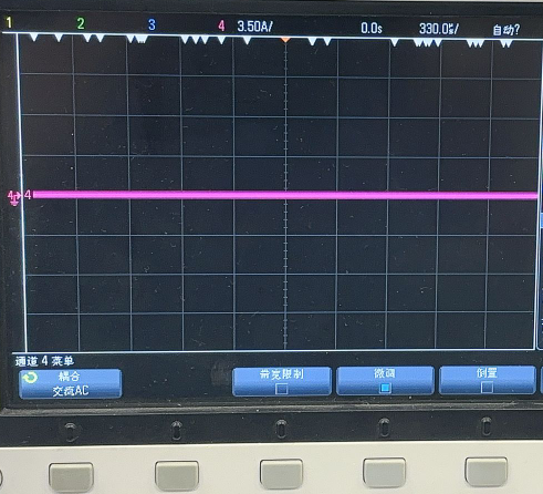
In response to the ripple caused by the switching power supply, the improvement approximates a clean straight line.