
How to reduce the ripple of BOOST boost circuit

When debugging the BOOST boost circuit, it can be found that the output ripple is large, and excessive ripple not only causes voltage instability, interferes with precision analog circuits, causes ADC sampling errors, but also exacerbates EMI radiation and even leads to system logic disorder. The ripple problem is essentially the result of the combined action of power device switching, energy storage component parameters, PCB parasitic effects, and control loops. So how to reduce ripple.
The core of high ripple in BOOST boost circuits is due to insufficient output capacitor filtering, suboptimal control loop/feedback, high inductance ripple, and PCB parasitic parameters. Improvement requires targeted solutions from four core dimensions: component selection, PCB layout, control, and compensation to control ripple within the specified range. This article mainly introduces how to reduce ripple from the following two points:
1. Component optimization: Increase output capacitance
Prioritize optimizing component selection and matching to reduce ripple from the source. Low ESR solid-state electrolytic capacitors and MLCC ceramic capacitors are selected as output capacitors, with a "large capacity+small capacity" parallel connection. The large capacity filters low-frequency ripples, while the 0.1~0.01 μ F high-frequency MLCC filters high-frequency burrs tightly against the output terminal. When the output ripple is too large, you can try increasing the output capacitor.
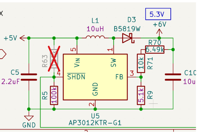
For example, when using AP3012 for boosting, the output ripple tested is 40mVpp
Boost circuit
Output ripple
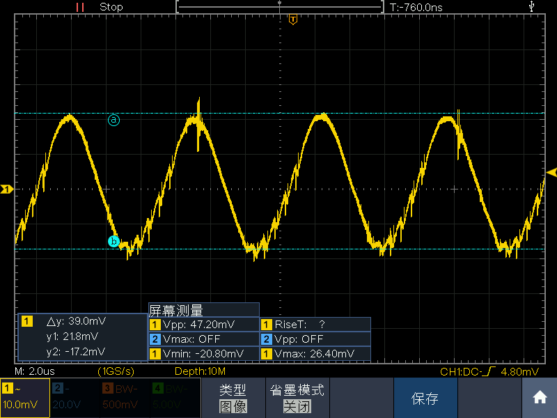
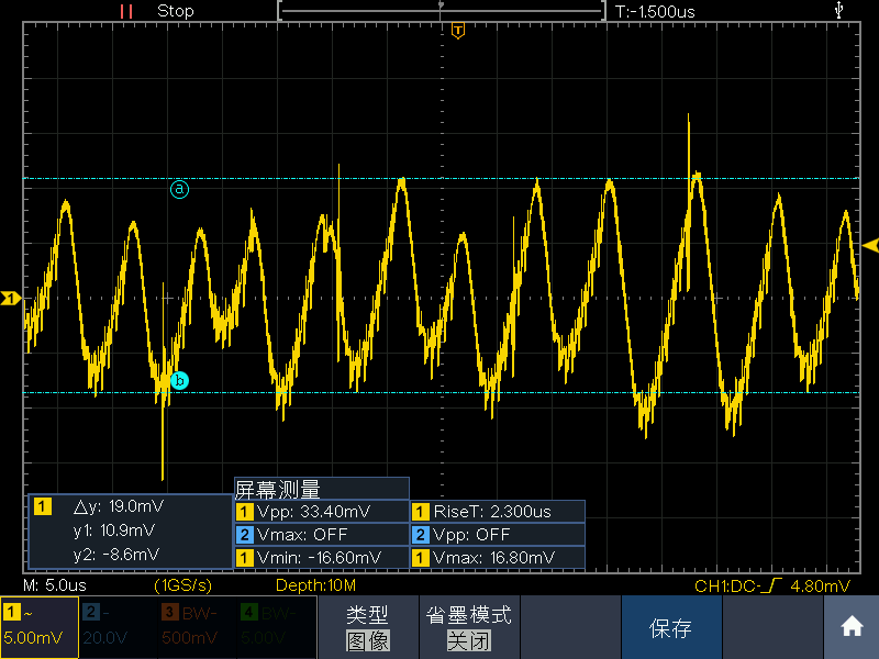
When the output capacitance is changed from 10uf to 22uf, it is evident that the output ripple has decreased, from around 40mVpp to around 20mVpp.
Output ripple
2. Optimize feedback loop
Feedback with feedforward capacitor (Cff) can optimize the high-frequency phase and gain characteristics of the loop, improve phase margin, and enhance system stability. By compensating for the zero and pole points of the loop, the transient response speed of the load is accelerated, and the duty cycle is quickly adjusted to correct the output voltage deviation, thereby reducing output ripple and voltage disturbance.
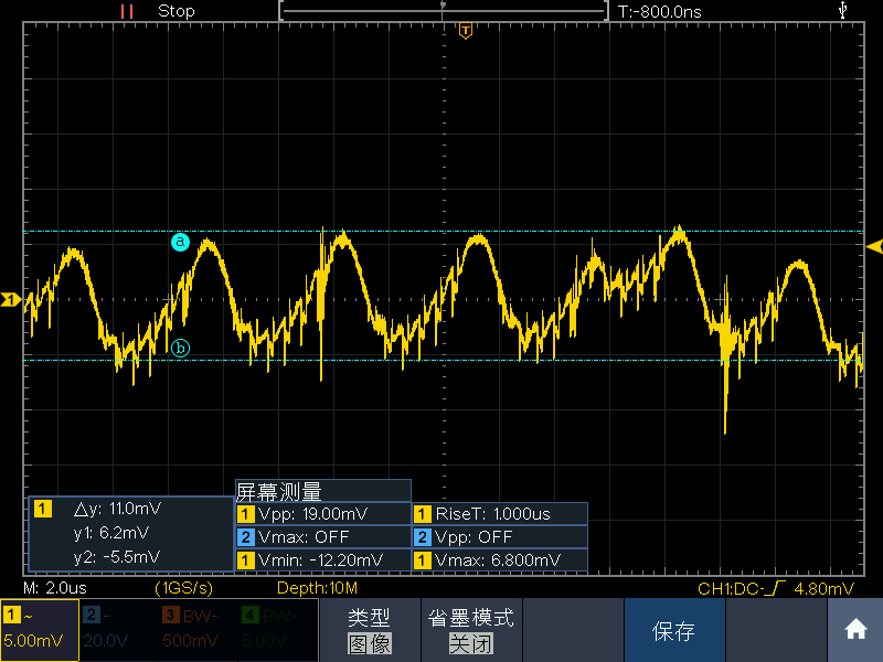
If a 47pf is added to R71 in Figure 1, the output ripple can be reduced to only about 11mVpp.
Output ripple
In summary, reducing the ripple of BOOST boost circuits requires a focus on components, circuits PCB、 By controlling the four core dimensions and implementing measures to optimize component selection and feedback loops without modifying the PCB, ripple can be stably controlled within design specifications while balancing efficiency and cost.