Analysis and Solutions for Bias Phenomena in Signal Testing

DC bias refers to an undesirable DC component that appears in sensors or electronic devices. Without an input signal, the output exhibits a certain DC voltage, resulting in a DC bias superimposed on the output signal when an input signal is applied. This DC bias may cause signal distortion, data errors, and degraded system performance. Therefore, appropriate corrective measures must be implemented.
DC bias may be caused by various factors, such as circuit issues, system malfunctions, or external sources. In analog audio systems, DC bias may originate from various sources, including capacitor failure, wiring imbalance, or improper amplifier design. In digital audio systems, DC bias may be caused by quantization error, bias circuits, or improper grounding. A common cause of DC bias is amplifier circuits.
Under ideal conditions, if the voltages at both input terminals of an operational amplifier are exactly the same, the output should be 0 V. In practice, a small differential voltage must also be applied at the input to force the output to zero. This voltage is referred to as the input offset voltage VOS. The input offset voltage can be regarded as a voltage source VOS, as shown in Figure 1-1.
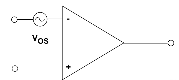
Figure 1-1 Input Offset Voltage
If a differential amplifier circuit is present in the design, the original signal carries the same DC voltage. The differential amplifier filters out the common-mode component and amplifies the differential-mode signal. However, the output may still exhibit some common-mode voltage. This is primarily because the operational amplifier can't completely filter out the common-mode component. It possesses a parameter called the common-mode rejection ratio (CMRR) to evaluate the amplifier's ability to suppress common-mode voltages. Generally, the higher the CMRR, the better the suppression effect, as shown in the common-mode circuit in Figure 1-2.
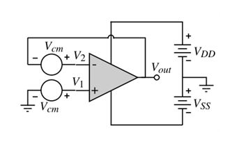
Figure 1-2 Common-Mode Circuit
Actual operational amplifiers exhibit multiple parameters, such as input offset voltage and common-mode rejection ratio, among others. These factors can all cause DC bias. The actual parameters of the OPA277 operational amplifier are shown in Figures 2-1 and 2-2.

Figure 2-1 Input Offset Voltage

Figure 2-2 Common-Mode Rejection Ratio
How to Eliminate DC BiasIn practical applications, numerous methods exist to eliminate DC bias, ensuring the signal remains more stable near zero. For example:
●Reference Voltage Method: By adding an adjustable reference voltage and superimposing it with the signal, DC bias compensation is achieved.
●Digital Filtering Method: Design filtering algorithms to eliminate or suppress the DC component in signals.
●DC Isolation Method: Separates DC components from the signal using components such as coupling capacitors or transformers to achieve DC offset correction.
When designing with a single operational amplifier, two offset pins are often reserved. These can be manually adjusted using an external variable resistor to symmetrically align the amplifier's two input terminals, thereby achieving zero offset.
In design, the reference voltage method is often employed to eliminate DC bias. This is because digital filtering techniques can actually impact the signal bandwidth, thereby affecting the testing of the original signal. Meanwhile, the frequency response when using coupling capacitors is influenced by the capacitance value, potentially causing attenuation of low-frequency signals.
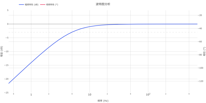
When using the AC coupling function of an oscilloscope to remove DC components, this is essentially achieved by inserting a coupling capacitor before the amplifier in the oscilloscope channel, which functions as a high-pass filter. The response of an oscilloscope's AC coupling is a first-order response, meaning that the amplitude-frequency and phase-frequency responses are affected across a wide bandwidth near the cutoff frequency. This may introduce distortion when observing signals with complex frequency components.
The cutoff frequency for AC coupling in standard oscilloscopes is typically below 10 Hz, generally around 5 Hz. Figure 2-3 shows the amplitude-frequency response curve of an ideal first-order RC filter. If the signal frequency is too low, attenuation will occur.